 TheCircuitDog
PCB Grounding and Return Paths
A return path completes every signal-current loop. Most PCB “grounding problems” are really unwanted current loops or disrupted return paths.
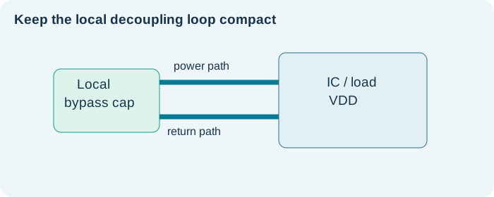
High-frequency return current follows the field
With a continuous reference plane, high-frequency return current tends to flow near the signal trace because that minimizes loop inductance.
Watch crossings over split planes
When a trace crosses a void or split, return current detours, increasing loop area and potentially creating noise or emissions. Route with continuous references where feasible.
Power and digital returns interact
Large load currents through a shared impedance can shift local ground potential. Carefully place sensitive ADC reference and analog front-end returns according to system-level guidance.
Measure instead of assuming
A long oscilloscope ground lead can create artifacts. Use low-inductance probing techniques when examining ripple, fast edges or voltage droop.
Practical checklist
- Identify each signal reference plane.
- Check plane splits under high-speed nets.
- Keep switching loops compact.
- Avoid shared impedance for noisy and sensitive returns where feasible.
- Probe supply at the load.