 TheCircuitDog
PCB & layout
PCB Trace Width vs Resistance and Heating
A PCB trace’s DC resistance is straightforward to calculate, but its allowable current depends on the board stackup, thermal environment and layout.
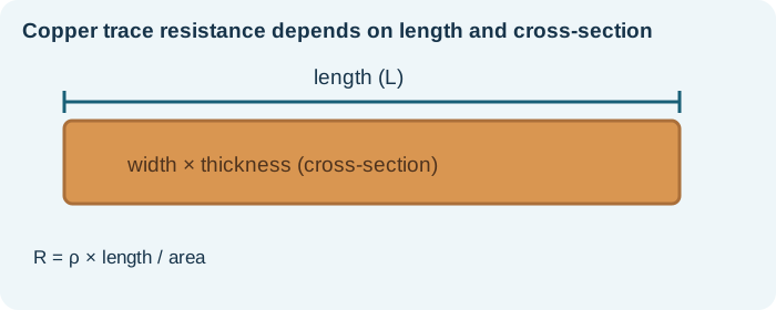
Resistance is geometry plus resistivity
DC resistance is ρL/(wt). Wider or thicker copper reduces resistance, while longer traces increase it.
Heat is I²R, but temperature rise is not
The trace dissipates power that must be carried away through copper, laminate, air and nearby copper areas. Two traces with equal resistance can have very different temperature rise.
Temperature changes the copper resistance
The room-temperature resistivity is only a starting point. Real copper resistance generally rises as temperature rises.
Use established design guidance
For current capacity, use applicable IPC-2152-based methods and validated thermal analysis or tests rather than a simple resistance equation alone.
Practical checklist
- Specify copper thickness and finished trace width.
- Measure effective path length.
- Include vias and connectors.
- Evaluate the thermal environment.
- Verify voltage drop and temperature rise.
Important: These are general educational procedures. Follow your lab safety requirements and device-specific datasheets, especially when working near dangerous voltages, high currents or stored energy.